§ 47 - PCB Creation
§ 47.1 - Overview
iToolBox can directly turn layered RGB images into printed circuit board CAM (Gerber) files. These files, in turn, may be used to manufacture printed circuit boards by a large number of printed circuit board vendors.
You might be asking yourself:
Why would I use an image processor to prepare circuit boards?
There are several possible reasons:
- There is the significant degree of freedom you gain in creating your various board layers; you can literally put anything you want on a printed circuit board.
- Another reason might be because you're familiar with iToolBox and don't particularly want to learn how to use — or purchase — a dedicated CAD system.
- Perhaps it appeals to you that by using iToolBox's layering technology, you can make your printed circuit boards look pretty much any way you want as you edit, when you print, and so on.
- iToolBox is free.
- Finally, while autorouting certainly has its good points, there is no autorouter in the world that can compete with the human mind for clever trace arrangement when the person creating the layout knows what they're doing.
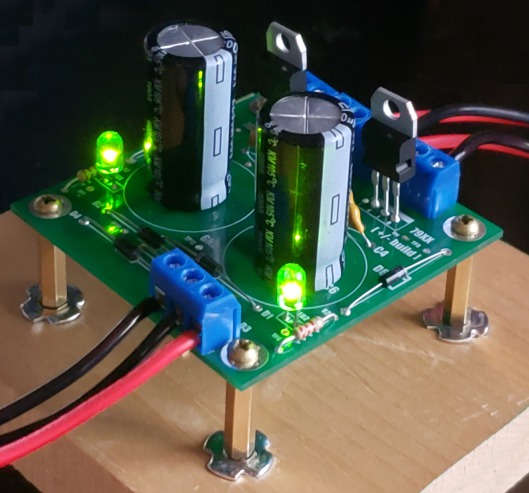
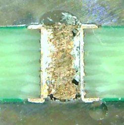
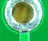 Microscopic view of printed circuit board designed in iToolBox production board manufactured by Chinese PCB house ALLPCB .063 pad, .015 trace, .031 hole .004 solder mask clearance |
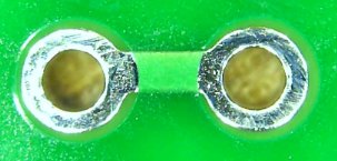 Microscopic view of printed circuit board designed in iToolBox production board manufactured by Chinese PCB house WELLPCB .060 pads, .025 trace, .031 holes .004 solder mask clearance |
Transverse cut through a via in board manufactured by Chinese PCB house WELLPCB
Note the consistent plating depth and application
The process is straightforward; it involves:
- Creating a printed circuit board (a type of layered image) using the New PCB dialog
-
Adding pads, vias and soldermask patterns using tools like
the Pad operator, the Plane operator, and the Valves operator - Adding connecting traces between components
- Creating legends for the electronic components
- Exporting the resulting board to Gerber file format with the Gerber Export dialog
The layered image created via the New PCB dialog is made up of like-sized layers in the following layer modes:
These layer types have several inherent characteristics that assist with creating printed circuit board artwork; all PCB art destined for Gerber file output must be created on these specific layer types.
§ 47.2 - Specific Uses of Color in a Gerber-Ready PCB Image Layer
Gerber file export produces a bi-level CAM file in all cases. Either there is layer information indicating copper or silkscreen or other information, or there is not. There are no levels of intensity involved in this process.
When you're creating board layers for this purpose, make sure that...
- Where you don't want copper plating, component legends, silkscreen rendering, solder-masking, or the board outline, ensure that all three of the RGB channels of your image are greater than half-intensity.
- Where you do want such output, at least one of the red, green or blue components must be less than half-intensity.
These levels are used to trigger output of the appropriate levels in the Gerber files.
The Pad operator enforces color selections that will generate output, so as long as you use it to generate your component pads, circuit vias, and solder mask, they'll be correct.
However, when creating traces with the Brushstroke operator operator or the Color Fill operator, and legends using the text or other Areatools, you need to firmly keep in mind the above restrictions on color.
This approach allows you to use a wide variety of colors in your printed circuit board layers. Any pixel color that has all three of its components above 1/2 intensity will result in no corresponding output at that position on the board.
White (255,255,255) is a canonical example; all three channels are as far above half intensity (128) as it is possible to go, and therefore, there will be no output where the pixels are white.
Likewise, black is zero-intensity in all three of the RGB channels (0,0,0), and so it will produce output in the Gerber files.
Another example is bright green (0,255,0), where the green channel is maximum, but the blue and red channels are minimum. This color will produce output, because it meets the criteria of having at least one channel below half-intensity (128 for 256 level colors as indicated in the Color Fill operator.)
Here are some further examples; remember, anything below 128 produces output:
| Example Color | Color Components | Gerber File Output State |
|---|---|---|
| █ | (0,0,0) | Will produce output |
| █ | (255,255,255) | Will not produce output |
| █ | (255,0,0) | Will produce output |
| █ | (0,255,0) | Will produce output |
| █ | (0,0,255) | Will produce output |
| █ | (255,0,255) | Will produce output |
| █ | (0,255,255) | Will produce output |
| █ | (255,255,0) | Will produce output |
| █ | (255,129,129) | Will not produce output |
| █ | (129,255,129) | Will not produce output |
| █ | (255,112,112) | Will produce output |
| █ | (112,255,112) | Will produce output |
Your image may incorporate transparency or not as you see fit; transparency is not used to control Gerber file output in any way, only the RGB color levels affect the final rendering. Using transparency with a layered image can help create more useful composites.
§ 47.3 - Antialiasing Disabled
§ 47.4 - Odd and Even Sized PCB Elements
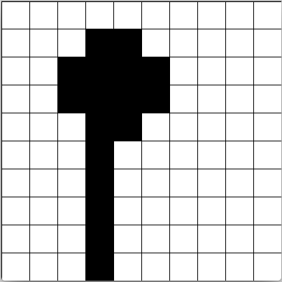
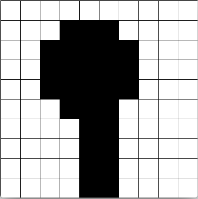
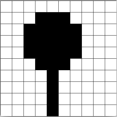
When you use the Brushstroke operator to stroke your printed circuit board traces, then you may want to either use odd-sized pads and odd-sized brushes to generate your traces, or even-sized pads and even-size brushes to generate your traces.
This is because the Brushstroke operator will try to center the trace brush over the path you set, and if the trace brush is of an even width and height and the pad is odd-sized, that is impossible to do because there is no center pixel in the trace brush.
Consequently, even-sized trace brushes can never be on-center with odd-width pads, they'll always be one pixel (1 mil) off.
The reverse is also true: odd-sized trace brushes can never be on-center with even-width pads, they'll also always be one pixel (1 mil) off. So the best practice is to use all even widths, or all odd widths.
A one pixel offset will not be technically significant in the vast majority of printed circuit board designs, so this being a concern mostly depends on just how picky you want to be.
The following examples should help to make this issue clearer:
§ 47.5 - A Walk-through Creating a Tiny Board
We'll create a tiny (and silly, but educational) printed circuit board.
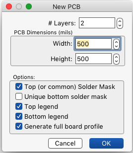
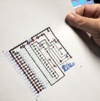
The first thing to do is create a 1/2 inch square blank board using the New PCB dialog. Open it using File/New PCB , and set it up like this:
After clicking the OK button a layered image will be generated that has all the layers you need for your printed circuit board, each in the appropriate layer mode. iToolBox uses special layer modes to control how operators such as the Pad operator apply information to the printed circuit board.
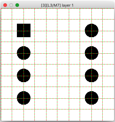
§ 47.5.1 - Placing a DIP IC on the PCB
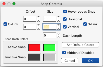
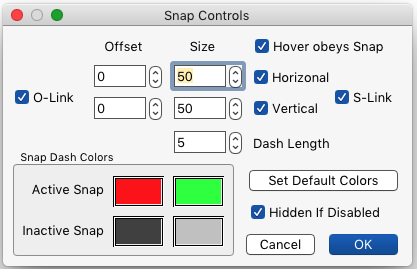
Now let's drop an 8-bit DIP into the board. First, open the Snap dialog using Selections/Snap Dialog , and set it up like this:
Now select the Pad operator, and use the Presets ⇳ menu to pick:
8-Pin DIP (.060.031 pads @ .300)) ⇳
Ensure that the Pad operator's ✓ Vertical control is checked.
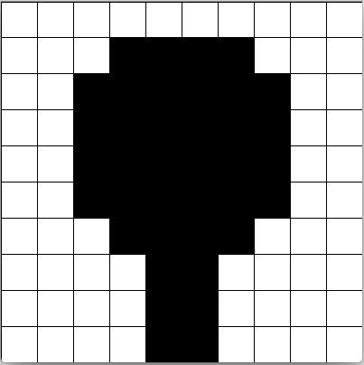
At this point, with the snap grid visible and turned on (on and off are controlled by Selections/Toggle Snapping , and display is controlled by Selections/Toggle Snap Display ), the master image of the printed circuit board should look like this (except for the arrow and the text):
With the rectangle selected, click on the first snap grid intersection at the top left of the master image as indicated above. This is the result you will get:
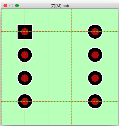
You now have a printed circuit board with a DIP IC layout on it. Look at all the image layers; you can see the pads, the drill holes, and the solder mask have all been set up for you by the Pad operator.
§ 47.5.2 - Creating Circuit Traces
Circuit traces can, technically speaking, be any shape or size. However, for small signals, you'll probably want them to be somewhere around the 10-mil range, with a similar minimum spacing between the traces.
This will generally ensure that your traces can be reliably manufactured. You can use any tool to create traces; what I like to do is create a round brush of the appropriate width using the New Image dialog and then the Brushstroke operator with the Areatools open figure option selected to actually create the trace path. I prefer 9 mil traces:
9 mil (9x9 pixel) brush for creating 9-mil traces
This brush has white non-stroking pixels, black stroking pixels, and
0-level alpha transparency to give it its (very) rough circular shape.
Re-open the Snap dialog with Selections/Snap Dialog and change it to 50 pixels (mils) as shown here:
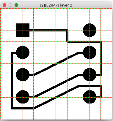
Then, use the Brushstroke operator and the polygon tool, with open figure selected so the brushstroke won't close the path, to create the following trace with six clicks on the snap grid in the layer 2 copper layer:
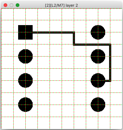
Example circuit trace on 50 mil centers
Rounded corners result from using a brush to stroke the trace's path
The next image demonstrates the creation of nicely parallel angled traces; but feel free to experiment:
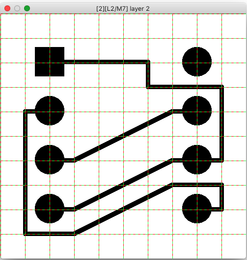
Example angled circuit traces on 50 mil centers
Rounded corners result from using a brush to stroke the trace's path
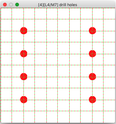
§ 47.5.3 - The Drill-hole Layer
Drill layers are special in several ways. First, the pad shapes used in the image are not what gets sent to manufacturing. Instead, iToolBox measures their height and width, takes the maximum dimension of the two, and then emits the appropriate drilling information to the drill output Gerber file.
Also, drill layers must only contain drill indicators.
Each printed circuit board manufacturer will have standard drill sizes; I like to use .031 drill holes for ICs, and this is usually available (but be sure to check — assumption is the mother of "try again, but with more information.")
§ 47.5.4 - Stacking up the Results
Now the layers stack up to make a basic printed circuit board:

§ 47.5.5 - The Legend (silkscreen) Layers
Remember, any color can be used for any layer element as long as at least one of its RGB channels is zero. So I'm going to create the silkscreen elements using a hot blue.
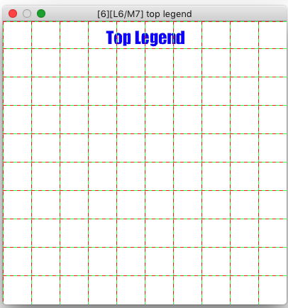
I'll use the text tool, set to a saturated blue (0,0,255) and the Impact font at 30 point size (you probably want larger text for aa production board; I'm just keeping it small to fit nicely on the example here) to create the designation "Top Legend". Finally, I'll use the Place operator's Top Center ⇳ setting with one click of the entire image tool to drop that in the image.

Next, we'll create silkscreen information for the bottom of the board. The trick here is to realize that the board, as worked upon and generated to a gerber CAM file, is always viewed from the top — but once produced, the bottom of the board will be viewed when flipped over, so all the legend work on it has to be reversed.
So to accomplish that, I'll first use the Layers dialog's H button to horizontally reverse all the layers of the circuit board so I can work on it from the bottom point of view:

Then I'll use the Place operator to drop the text into the bottom legend layer at the bottom center:
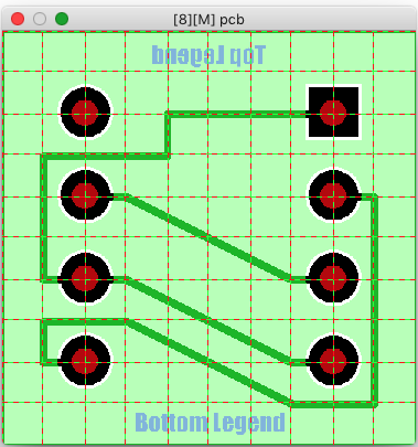
Finally, I'll flip the image back to its normal orientation (as viewed from the top) using the Layers dialog's H control again:
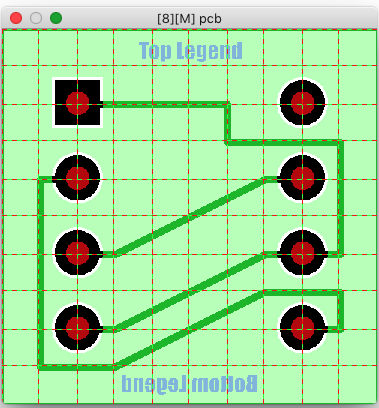
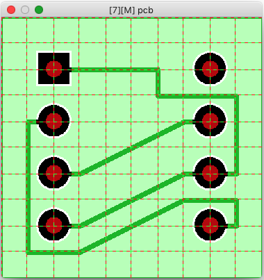
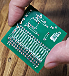
The sample board is now complete.
§ 47.6 - Printing a Single Layer or the Master
When printing, the image DPI should be set first depending on your goals.
The critical thing to keep in mind is that the printed circuit board layers are 1 mil (one thousandth of an inch) per-pixel.
Some examples:
For a 100% resolution (1:1) printout, set the DPI of the image to 1000 on both X and Y with the DPI operator.
For a 50% resolution (1:2) printout, set the DPI of the image to 2000 on both X and Y with the DPI operator.
For a 200% resolution (2:1) printout, set the DPI of the image to 500 on both X and Y with the DPI operator.
Once you have set the image DPI, you are ready to print.
§ 47.7 - Creating the Gerber Files
Each layer here gets a specific treatment when generating the Gerber file output. We'll walk though each one.
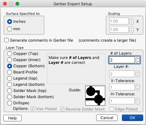
§ 47.7.1 - The Circuit Side Layer
Make the circuit layer (layer 2) the action image by -clicking on its titlebar, and then select File/Export Gerber Files
Select a reasonable file name that ends with .gbr
The # of Layers and Layer # settings are critical here. For a 2-sided board, the top (component) layer will automatically be set to 1 and the bottom (circuit) layer automatically set to 2. For a board with more than 2 layers, the top layer is automatically set to 1, the bottom layer is set to the last layer number (in other words, if this is an 8-layer board, the bottom layer will be automatically set to 8.) However, for the board's inner layers, you are responsible for setting the layer number correctly.
Set the Gerber file dialog up as follows, then select OK:
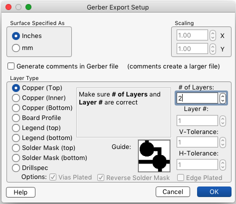
§ 47.7.2 - The Component Side Layer
Make the component layer (layer 1) the action image by -clicking on its titlebar, and then select File/Export Gerber Files
Select a (different) reasonable file name that ends with .gbr
The # of Layers and Layer # settings are also critical here. For a 2-sided board, the top (component) layer will automatically be set to 1 and the bottom (circuit) layer automatically set to 2. For a board with more than 2 layers, the top layer is automatically set to 1, the bottom layer is set to the last layer number (in other words, if this is an 8-layer board, the bottom layer will be automatically set to 8.) However, for the board's inner layers, you are responsible for setting the layer number correctly.
Set the Gerber file dialog up as follows, then select OK:
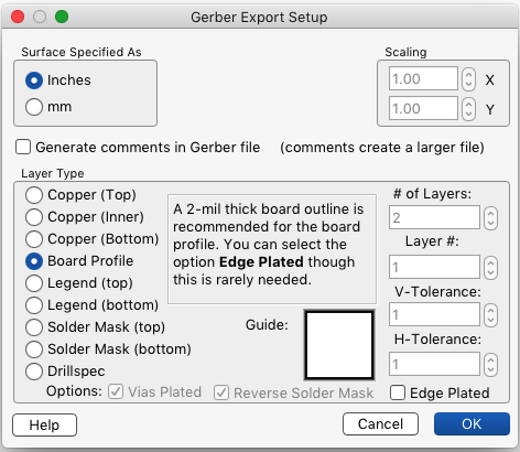
§ 47.7.3 - The Board Outline (Profile) Layer
Make the board outline layer the action image by -clicking on its titlebar, and then select File/Export Gerber Files
An available option here is to have the cut sides of the board plated. This can be useful in some cases, and I'm sure if your case is one of those, you'll know it. 
Select a (different) reasonable file name that ends with .gbr and then set the Gerber file dialog up as follows, then select OK:
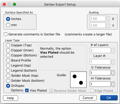
§ 47.7.4 - The Drill Layer
Speaking with my engineer's hat screwed on tightly, my advice is always make a single sided board as double sided with component side pads and plated-through holes.
Make the drill layer the action image by -clicking on its titlebar, and then select File/Export Gerber Files
Select a (different) reasonable file name that ends with .gbr and then set the Gerber file dialog up as follows, then select OK:
§ 47.7.5 - The Top Solder Mask Layer
To repeat myself in a good cause, you almost certainly want pads on both side of tha board (and plated through holes) in every design, and consequently you also want a top-of-board solder mask layer as shown here, but it's up to you.
For the demo, I do want solder masks — I always want them.
Make the solder mask layer the action image by -clicking on its titlebar, and then select File/Export Gerber Files
Select a (different) reasonable file name that ends with .gbr and then set the Gerber file dialog up as follows (make sure that ✓ Reverse Solder Mask is not checked, because we are using an actual plane of coverage, not just pads, to represent the solder mask), then select OK:

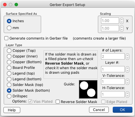
§ 47.7.6 - The Bottom Solder Mask Layer
With the the solder mask layer still the action image by -clicking on its titlebar, again select File/Export Gerber Files (we're going to create a second, identical mask for the other side of the board from the same layer... this is typical, but you can create a different mask if you are so inclined.)
Select a (different) reasonable file name that ends with .gbr and then set the Gerber file dialog up as follows, then select OK:
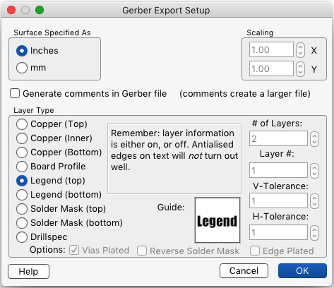
§ 47.7.7 - The Silkscreen (Top Legend) Layer
Make the top legend layer the action image by -clicking on its titlebar, and then select File/Export Gerber Files
Select a (different) reasonable file name that ends with .gbr and then set the Gerber file dialog up as follows, then select OK:
§ 47.7.8 - The Bottom Legend Layer
Make the bottom legend layer the action image by -clicking on its titlebar, and then select File/Export Gerber Files
Select a (different) reasonable file name that ends with .gbr and then set the Gerber file dialog up as follows, then select OK:
That's the whole process for a very typical, although small and silly, board. Most printed circuit board manufacturers will accept a .zip file containing all of the files you just produced, and should be able to manufacture your board without any more input on how it is to be made. Arrange a quantity, a price and a shipping methodology, and you should be good to go.
§ 47.8 - Higher-Density Designs — Two Lines Between Pads
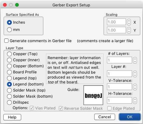
For a 2-lines-between-pads circuit density, I suggest a 59 mil pad diameter, with 8 mil traces between the pads. This allows for 8 or more mils spacing between pad edges and adjacent traces as the following image demonstrates:
Both 8 mil traces and 8 mil spacing are generally within most modern printed circuit board manufacturer's capabilities.
The trick here is getting the traces between the pads on-center, because there is no snap grid spacing that is divisible by both 8 and 100.
So I carefully create library objects like the one above, and then use them directly when I'm actually laying out a board.
From there, it's easy to connect to the traces that are needed, and then eliminate the ones that aren't using the wand.
The above image serves as a high-trace density template for an 8-pin DIP package; you are welcome to use it. You can easily generalize it into a 14-, 16- or 20-pin version as well.
You can draw anything you need at the time you need it, but I find the templates to be faster and generally more accurate, because I only have to get them right once.
I've marked the drill holes in the library item's trace layer here with a pure red .031 (31 pixel diameter) marker for my own convenience; this will not produce a gap in copper coverage, as the red color's RGB channel values are, respectively, 255, 0 and 0 — whenever even one of the channels is below 1/2 intensity, printed circuit board output is generated.
There's a benefit to do this as well; the pattern may be placed directly into the drill layer, then the black areas filled with white using the wand. At that point, we have correctly placed and sized drill holes for the special DIP IC.
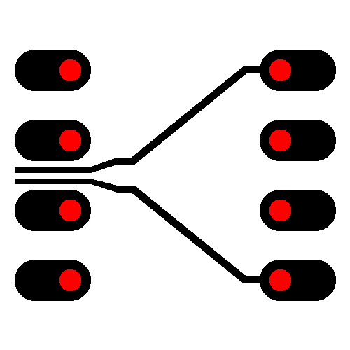
Here's an example of using 10 mil traces generally, but working with two lines at 8 mils between elongated-style pads...

...I used a ten-mil/pixel grid and a 10-mil/pixel brush with the polygon tool with open figure active with the Brushstroke operator to place the majority of the trace using four points, from the pad at the right, nearly up to the 8-mil trace I wanted to connect to. Then I used the Color Fill operator with the polygon tool with open figure inactive with the Color Fill operator set to black, and created an arbitrary shape connection between them.
Again, you can use whatever trace widths and pad sizes you prefer; I have used a variety of widths and pads in the examples on this page to demonstrate this. Just make sure that you're designing within the limits of the printed circuit board manufacturer you plan to use; that is what ultimately sets the constraints on what you can get away with in the printed circuit board manufacturing phase.
A quick and inexpensive way to get your boards manufactured is by using a Chinese printed circuit board manufacturer. I have worked with several of them, listed just below, and made sure that they can produce quality printed circuit boards from the Gerber files output by iToolBox:
| ALLPCB | https://www.allpcb.com |
| OURPCB | https://www.ourpcb.com |
| WELLPCB | https://www.wellpcb.com |
, Previous Page . Next Page
t TOC i Index k Keyboard o Operators g Glossary c Changes
![]()
on February 27th, 2026 at 17:38 MT
| Please consider supporting my iToolBox development efforts with a small PayPal donation. |