Layers Dialog — .elx Files / Layer Blending Modes / PCB Blend Modes
This manual was generated with wtfm
on February 27th, 2026 at 17:38 MT
wtfm uses aa_macro and SqLite
wtfm and aa_macro are coded in python 2.7
iToolBox 3.12
This Documentation and Associated Application Executables are Public Domain
§ 19.6.11.5 - PCB Board Profile
PCB (printed circuit board) Board Profile layers are always fully opaque — no layer below them will be visible in the master image. Layer content with any channel below half-intensity will be displayed verbatim in the layer stack and will be treated as board profile information by the Gerber file exporter; content above half intensity will be displayed in the layer stack as white (255,255,255) and ignored by the Gerber file exporter.
Caution: PCB Board Profile layers should always be placed at the bottom of the layer stack, and you should always have a PCB Board Profile layer in your printed circuit board layered image.
Tip: It is strongly recommended that board profiles are created with a 2-pixel (2 mils, or .002 inches) edge indication. Some CAM software cannot resolve a 1-mil board profile.
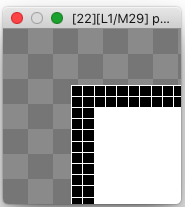
iToolBox's File/New PCB command automatically creates a 2-mil profile if you select ✓ Full Board Profile so this is only a concern if you create your own profile layer, or modify the one that iToolBox created for you.
PCB layer modes cannot incorporate positional offsets.
Note: Because the Gerber file CAM files are bi-level, there's no such thing as a partially-on level, no matter what. So when working on printed circuit board layer types, areatool antialiasing does not function, regardless of the actual setting of antialiasing for the particular areatool in use.
| See also: |
PCB Copper PCB Legend PCB Drill Holes PCB Solder Mask |

Document Keyboard Navigation
, Previous Page . Next Page
t TOC i Index k Keyboard o Operators g Glossary c Changes
, Previous Page . Next Page
t TOC i Index k Keyboard o Operators g Glossary c Changes
![]()
on February 27th, 2026 at 17:38 MT
| Please consider supporting my iToolBox development efforts with a small PayPal donation. |