§ 25 - New PCB Dialog
The New PCB dialog creates a layered image with the layers you need to design a printed circuit board.
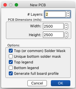
§ 25.1 - # Layers Control
# Layers controls how many copper layers there will be in the printed circuit board.
§ 25.2 - PCB Dimensions
This sets the Width and Height of the printed circuit board, in mils (thousandths of an inch.)
§ 25.3 - Options
Here, you select the non-copper layers you want in your design.
Each printed circuit board should have at least one solder mask layer (which you can use to generate both a top and bottom solder mask), or two if the top solder mask will be different from the bottom solder mask.
Each printed circuit board should have at least one legend layer; it is common to label components and connections on the top side of the board, but not the bottom. However, if you wish to create a second legend layer for the bottom of your printed circuit board, you can do that here.
Each printed circuit board should have a board profile layer. This layer is what tells the printed circuit board manufacturer how to shape and size the circuit board itself. Without this layer, they will not be able to manufacture your board. In addition, within the layered image, this layer provides a white backdrop that the rest of the printed circuit board layers are displayed over.
, Previous Page . Next Page
t TOC i Index k Keyboard o Operators g Glossary c Changes
![]()
on February 27th, 2026 at 17:38 MT
| Please consider supporting my iToolBox development efforts with a small PayPal donation. |