§ 12.11.65 - Pad
No Script Command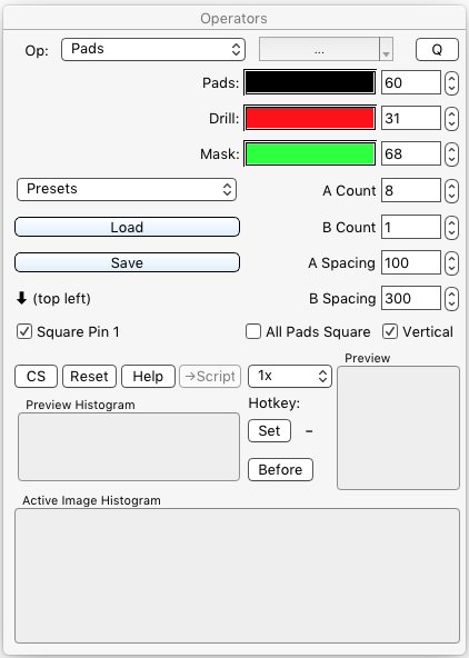
You should always use the rectangle tool to place pads or pad arrays. Single pads, or pin one of multiple pad arrays, will be placed at the center of any rectangle that is dragged out with the mouse; a single click without a subsequent drag will generate a center location at that specific pixel.
Using the Pad operator, you can create single pads, square or round; SIP and DIP pad arrays, and even pin-grid arrays.
There are three presets that will generate single pins; they create .060, .075 and .100 round or square pins. You select if the pin is round or square with the ✓ Square Pin 1 control. You can change any of the Pads, Drill or Mask (solder mask) sizes manually as well in order to create a single pad of any size.
Each of the generated layer components of a pad will generate in its own color, on the appropriate layer(s.) You can select different colors by left-clicking on the color well.
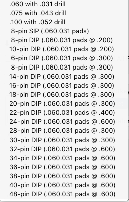
You can create SIP and DIP packages using the available presets, or you can create any custom SIP, DIP or pin-grid array style by setting the A Count, B Count, A Spacing, B Spacing ✓ Square Pin 1 and ✓ All Pads Square controls individually. You can save custom styles using the Save button, and load them back using the Load button.
When you create a DIP, SIP or pin-grid array, you can specify that pin one be square using the ✓ Square Pin 1 control; or you can make all the pins square by selecting the ✓ All Pads Square control.
DIPs, SIPs and pin-grid arrays may be oriented vertically (with pin one up and left) or horizontally (with pin one down and left.) All pad arrays are generated starting at pin one, which will be located at the center of the rectangle you drag out or at the specific pixel if you only click rather than drag out a rectangle.
Immediately after a pad or a pad array has been generated, with the Pad operator still selected, the undo command will undo all the affected layers. If you need to undo more than one pad placement, or the Pad operator is no longer the selected operator, then use U (shift+u) to force an undo on all printed circuit board layers. Be careful with this; if individual operations have been carried out on single layers, the undo operation will not do exactly what you expect.
§ 12.11.65.1 - An Example Pin Grid Array
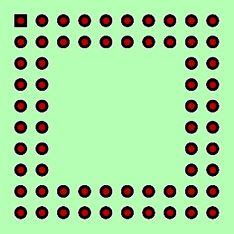
To create this exact array:
-
Generate the 10x10 array
- check ✓ Pin One Square
- check ✓ Vertical
- Pads = 60
- Drill = 31
- Mask = 68
- A Count = 10
- B Count = 10
- A Spacing = 100
- B Spacing = 100
- Using the rectangle tool, click where you want pin one (the top left pin) located
- Remove the 36 (inner 6x6) inner pads with the Layer Clear operator using the rectangle areatool
| See also: |
PCB Copper PCB Legend PCB Drill Holes PCB Solder Mask PCB Board Profile The Valves operator The Plane operator The Layer Clear operator |
, Previous Page . Next Page
t TOC i Index k Keyboard o Operators g Glossary c Changes
![]()
on February 27th, 2026 at 17:38 MT
| Please consider supporting my iToolBox development efforts with a small PayPal donation. |